Decoder logic circuit diagram and operation
Last Updated on November 12, 2022 by Engr. Shahzada Fahad
Table of Contents
Decoder logic circuit diagram and operation
A decoder is a type of logic circuit, which converts binary numbers (or binary inputs) to decimal numbers (or decimal outputs). A decoder is actually a code translator, which consists of multiple inputs and outputs and by means of which, some specific number can also be determined. In other words, a decoder is a combinational logic circuit, which detects the presence of a word or binary number. Its input is a parallel binary signal while its output is a single binary signal, which represents the presence or non–presence of a particular binary number. Remember that circuits, both of demultiplexer and decoder are analogous (or decoder and demultiplexer both are similar) except that data input or enabled input or data line does not exist in a decoder and control input bits produce an active output line (i.e. decoder provides just one output at a given time)
We know that information in digital systems is represented by means of binary codes. A “n” bits binary code is capable of 2n binary elements of a coded information. As such, a decoder is a combinational circuit, which changes binary information via “n” input lines up to a maximum of 2n output lines. The basic function of a decoder is to ascertain the presence of a distinct combination of its input bits (code) and reveal the presence of this code via a certain output level. A decoder generally consists on “n” input lines for control or handling of “n” bits and one 2n output lines for showing the presence of one or more “n” bit combinations. Decoders are mostly used in computers, calculators and digital clocks etc. As decoders are used for converting binary numbers into decimal numbers, therefore they are normally mounted on the output stage of a digital circuit. Remember that AND gates are applied in a decoder circuit. As output of an AND gate is binary 1 when all its inputs are also binary 1, thus presence or existence of any binary number can be determined by connecting the input of AND gate with its source in an accurate manner.
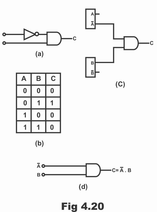
In figure 4.20 (a), an AND gate consisting of a two–inputs AND gate has been demonstrated, which detects the presence of binary number 01. The number which is desired to be detected comprises two bits A and B. When the value of A is 0 and the value of B is 1, both inputs of AND gate are high or binary 1, thus output C becomes binary 1. It determines the presence of the number 01. In figure, an inverter has been mounted alongside A input, which changes the top input of AND gate (i.e. binary 0) to binary 1. However, the decoders’ output for the remaining pairs (i.e. 11 and 1000) of both bits present on input, is zero. As has been demonstrated via a truth table shown in figure (b). In this manner, the presence of binary number 01 is determined by means of a decoder. In figure (c), binary input number has been obtained from a flip–flop register, and AND gate has been shown to determining the presence of binary number 01. As complement outputs are received by means of flip–flop, therefore there is no need for the application of an inverter. When flip–flop A is resets and flip–flop B sets, then binary number 01 is stored on the register. Therefore, A and B outputs of the register are high at that time. In such a situation, decoder AND gate output is high. Remember that for simplicity purposes, inputs source (i.e. register) of the AND gate is not shown in the diagram. In figure (d), just one input state has been shown on gates’ input and its output has been exemplified via a Boolean expression (i.e. source has not been illustrated on the circuit).
It has to be kept in mind that AND gate can be used in order to determine presence of a binary number of any size. In such a situation, the number of gate’s inputs equals to the total number of bits present in a binary word.
Figure 4.20
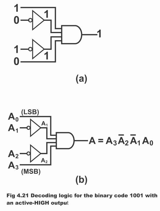
Suppose that we want to know when does a binary 1001 exist on the inputs of a digital circuit (i.e. we want to determine the presence of a 4 – bit number 1001). As output of AND gate is high at a time when all of its inputs are high, therefore an AND gate can be used as a basic decoding element. Therefore, we must be confident that all inputs of an AND gate are high at a time when binary 1001 occurs. If the mid–two bits (i.e. 0s) are inverted, this can become possible. (figure 4.21 (a). The logic equation of decoder as shown in figure (a), has been illustrated via the figure (b). Remember that output of a decoder for all possible combinations of 4 – bits (A0 A1 A2 A3 = 1001) existing inputs, is zero. In other words, when A0 = 1, A1 = 0, A2 = 0 and A3 = 1 values are provided on AND gate, its output becomes high or 1. However, with the exception of this particular situation, output of AND gate will be low or zero in all other situations.
Figure 4.21 – decoding logic for the binary code 1001 with an active – high output
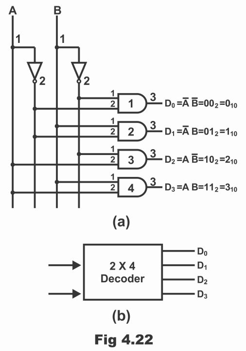
Apart from determining the presence of a binary word through a decoder, most often existence of possible states or numbers formed via input of a binary word, can also be ascertained. For example, 4 different pairs can be formed via a 2 – bit input word (i.e. 20 = 22 = 4). Practically, an operative decoder can detect the presence of all these different pairs (combinations). For clarity purposes, a 2 to 4 lines decoder has been reflected with its block diagram in figure 4.22., which has been decoding two inputs A and B into four possible outputs D0, D1, D2 and D3. Here, four AND gates are used for decoding four possible input conditions. The process to decode these 4 – possible input states resulting from 2 – binary input lines and 4 – possible outputs resulting from these input states, has been exemplified via a truth table shown in figure 4.23. Remember that only one output exists for every binary combination. As only one output of four outputs available on the circuit at a given time is high, that’s the reason it is also known as a 1 – off – 4 decoders. Decoders are available in markets in the form of ICs, some types of which are as follows:
74139 → 2-to -4-line decoder
74138 → 3-to-8-line decoder
74154 → 4-to-16-line decoder
Figure 4.22 – (a)
74139 → 2-to -4-line decoder
Figure 4.23 – truth table of 2 – to – 4 – line decoder
| Inputs | Outputs | ||||
| A | B | D0 | D1 | D2 | D3 |
| 0 | 0 | 1 | 0 | 0 | 0 |
| 0 | 1 | 0 | 1 | 0 | 0 |
| 1 | 0 | 0 | 0 | 1 | 0 |
| 1 | 1 | 0 | 0 | 0 | 1 |
Operation
The process of this decoder can better be inculcated via a truth table illustrated in figure 4.23
- When both inputs A and B are low, only D0 output is high, which indicates the presence of binary 00 on inputs (i.e. gate number 1 decodes binary 00 inputs), whereas all remaining inputs in such a situation are low (because any one of the inputs of gate number 2,3 or 4 essentially becomes zero or low, owing to which, these three gates become disabled)
- When value of A is 0 and B is 1, i.e. A = 0 and B = 1, only of the four gates i.e. gate number 2 has both high (or 1) inputs, whereas at least any one input of rest of the gates is low or zero, due to which only D1 output is high, which informs about the presence of binary 01 on inputs.
- When values of AB are binary 10 i.e. AB = 10, in such a situation, all outputs except D2 are low.
- When both inputs A and B are high, except gate number 4, all other gates by means of one or both low inputs, provide low output. And only gate number 4 by means of both its high inputs, provides high output in the form of D3 and informs about the presence of binary number 11 on inputs.
Remember that decoder circuit displayed in the figure can also be seen as a binary to decimal converter, i.e. it converts binary input to such output, which represents any one decimal number from 0, 1, 2 or 3.
In other words, output line value of which is 1, represents binary number found on its input along with an equivalent decimal number. For instance, if a bulb is fitted with every output, when bulb D0 irradiates, it means that binary number 00 exists on input and decimal number 0 exists on output. Similarly, in case of presence of binary number 01, 10 and 11 on inputs, bulbs D1, D2 and D3 irradiate, which represent 1, 2 and 3 on output respectively.
74138 → 3-to-8-line decoder
For further explanation, a 3- to – 8 – line decoder has been demonstrated in figure 4.24, the operation of which has also been exemplified via a truth table as shown in figure 4.25. A 3 – to – 8 – line decoder means that this decoder has 3 inputs and it decodes these three inputs into 8 outputs. Further, each of its outputs represents decimal numbers equivalent to 3 input variables provided to it. In this figure, 3 inverters have been illustrated, which provides a complement of inputs. Every gate out of a total number of 8 AND gates, represents a decimal number (because basic function of a decoder is to convert binary numbers to decimal numbers). However, the specific mission of this 3 – to – 8 – line decoder is to convert binary inputs to an octal.
It is evident from the operation of this decoder as illustrated via its truth table that during a given period of time, just one of its output equals to 1. The output line, value of which is equal to 1, represents decimal number equivalent to the binary number present on the input line. For example, if D2 output is equal to 1, it means that binary number 010 exists on input, equivalent decimal of which is 2. Similarly, a high output of D5 means decimal number 5 and D7 ‘s high output means decimal number 7.
Figure 4.24 – A 3 – to – 8 – line decoder
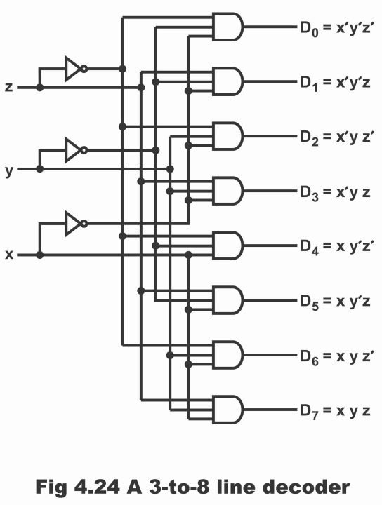
Figure 4.25 – truth table of a 3 – to – 8-line decoder
| Inputs | Outputs | |||||||||
| x | y | z | D0 | D1 | D2 | D3 | D4 | D5 | D6 | D7 |
| 0 | 0 | 0 | 1 | 0 | 0 | 0 | 0 | 0 | 0 | 0 |
| 0 | 0 | 1 | 0 | 1 | 0 | 0 | 0 | 0 | 0 | 0 |
| 0 | 1 | 0 | 0 | 0 | 1 | 0 | 0 | 0 | 0 | 0 |
| 0 | 1 | 1 | 0 | 0 | 0 | 1 | 0 | 0 | 0 | 0 |
| 1 | 0 | 0 | 0 | 0 | 0 | 0 | 1 | 0 | 0 | 0 |
| 1 | 0 | 1 | 0 | 0 | 0 | 0 | 0 | 1 | 0 | 0 |
| 1 | 1 | 0 | 0 | 0 | 0 | 0 | 0 | 0 | 1 | 0 |
| 1 | 1 | 1 | 0 | 0 | 0 | 0 | 0 | 0 | 0 | 1 |
BCD-to-Decimal Decoder
BCD (which is an abbreviation of the binary coded decimal)- BCD-to-decimal is a logic circuit, which can convert every BCD code (8421) to any one of the 10 possible decimal digits (0 – 9). It is generally known as a 4-line-to-10-line decoder or 1 of 10 decoder.
We know that largest and most common application of a decoder circuit is to convert binary numbers to equivalent decimal numbers. For this purpose, BCD to-decimal decoder is extensively used. The input of this decoder consists on a 9 – bit parallel binary word, which reflects first ten BCD numbers from 0000 to 1001. Thus, in order to represent first 10 BCD numbers 0 -9 into ten possible outputs, ten AND gates are used which analyze inputs and provide 10 possible outputs from 0 – 9 by means of decoding it. In other words, as a BCD code represents just 10 decimal numbers 0 – 9, therefore only 10 decoding gates are required for a BCD to decimal decoder circuit. In table shown via figure 4.26, a list of 10 BCD codes and its corresponding decoding functions has been given. Every decoding function of these decoding functions can be performed by means of application of NAND and AND gates. However, it must be kept in mind, that low output results by means of using NAND gates (because it is a feature of NAND gate that when all of its inputs are high, in such a situation it provides low output). And a high output is received by means of using AND gates (in other words, if high output is desired, AND gates are used for the purpose of decoding and in case active low output is required, a decoder circuit comprising NAND gate is applied)
Figure 4.26 – BCD decoding functions
| Decimal Digit | BCD Code
D C B A |
Decoding Function | ||||||
| 0 | 0 | 0 | 0 | 0 | D | C | B | A |
| 1 | 0 | 0 | 0 | 1 | D | C | B | A |
| 2 | 0 | 0 | 1 | 0 | D | C | B | A |
| 3 | 0 | 0 | 1 | 1 | D | C | B | A |
| 4 | 0 | 1 | 0 | 0 | D | C | B | A |
| 5 | 0 | 1 | 0 | 1 | D | C | B | A |
| 6 | 0 | 1 | 1 | 0 | D | C | B | A |
| 7 | 0 | 1 | 1 | 1 | D | C | B | A |
| 8 | 1 | 0 | 0 | D | C | B | A | |
| 9 | 1 | 0 | 0 | 1 | D | C | B | A |
When a BCD number is applied on a decoder’s input, one of ten output lines becomes high (in case of AND gate decoder circuit) which represent the presence of a specific BCD number on input. The output of such decoders is used in order to irradiate its corresponding decimal numbers, so that they could be easily read.
Another important point should be kept in mind about BCD that BCD digits are from 0000 to 1001 and all other digits above it (i.e. 1010 to 1111) are not included in BCD code, because the largest digit which can be included in a BCD code is 9.
In figure 4.27, a distinct BCD to decimal decoder circuit has been shown consisting of ten AND gates (it is also known as 1 of ten decoder because only one of its ten output lines is high). A 4 – bit BCD number (bits of which have been named as A, B, C and D) is applied on decoder’s input, which provides normal signals and complement signals by means of an inverter mounted alongside corresponding AND gate’s input, which decodes it. For example, when value of ABCD is 0011 i.e. ABCD = 0011, then inputs of Y3 gate only are high and any one input or more than one inputs of rest of the gates is low, as a result output only of Y3 is high. It means that BCD numbers existing on input are equal to equivalent decimal number 3.
Figure – 4.27 1 – of – 10 decoders
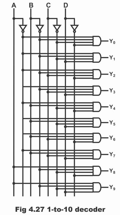
If value of ABCD is 1000 (i.e. ABCD = 1000), in such a situation, inputs of Y8 gate only are high as result of which, only Y8 gate receives high output. Similarly, if other possibilities of ABCD (0000 to 1001) are analyzed, it becomes evident that the gate which has high output, always represents equivalent decimal numbers of BCD numbers present on input.
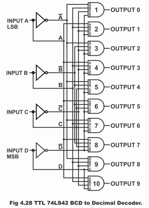
In figure 4.28, a peculiar BCD to decimal decoder has been displayed, which consists of NAND gates instead of ten AND gates. The BCD numbers (which consists of 4 – bits A, B, C and D) provided via inverters mounted on the decoders’ inputs produce complement and normal signals and transmit the same on NAND gate input for decoding it. Remember that in case the AND gates mounted on decoder circuit as shown in the figure 4.27 are replaced with NAND gates, this circuit will also become analogous to the circuit demonstrated in figure 4.28.
Figure 4.28 – TTL 74 LS 42 BCD to Decimal Decoder
The operational method of this decoder is as follows:
When value of the input BCD is 0000 i.e. ABCD = 0000, then all inputs of gate number 1 (which transmit towards gate via inverter), become high. As a result, gates’ output becomes zero (because when all inputs of a NAND gate are high or 1, its output is binary 0) whereas by means of at least one input of other gates being zero, its output becomes high. In other words, the gate which has been decoding on a particular state of gate input, output of all other gates with the exception of this particular gate, becomes high. Thus, a low or zero output is received, which represent an equivalent decimal number equal to the BCD code present on input. This has been illustrated in figure 4.29 via a BCD to decimal decoders truth table.
Figure 4.29 – Truth Table for BCD to Decimal Decoder
| No | BCD INPUT | DECIMAL OUTPUT | ||||||||||||
| D | C | B | A | 0 | 1 | 2 | 3 | 4 | 5 | 6 | 7 | 8 | 9 | |
| 0 | L | L | L | L | L | H | H | H | H | H | H | H | H | H |
| 1 | L | L | L | H | H | L | H | H | H | H | H | H | H | H |
| 2 | L | L | H | L | H | H | L | H | H | H | H | H | H | H |
| 3 | L | L | H | H | H | H | H | L | H | H | H | H | H | H |
| 4 | L | H | L | L | H | H | H | H | L | H | H | H | H | H |
| 5 | L | H | L | H | H | H | H | H | H | L | H | H | H | H |
| 6 | L | H | H | L | H | H | H | H | H | H | L | H | H | H |
| 7 | L | H | H | H | H | H | H | H | H | H | H | L | H | H |
| 8 | H | L | L | L | H | H | H | H | H | H | H | H | L | H |
| 9 | H | L | L | H | H | H | H | H | H | H | H | H | H | L |
| Invalid | H | L | H | L | H | H | H | H | H | H | H | H | H | H |
| Invalid | H | L | H | H | H | H | H | H | H | H | H | H | H | H |
| Invalid | H | H | L | L | H | H | H | H | H | H | H | H | H | H |
| Invalid | H | H | L | H | H | H | H | H | H | H | H | H | H | H |
| Invalid | H | H | H | L | H | H | H | H | H | H | H | H | H | H |
| Invalid | H | H | H | H | H | H | H | H | H | H | H | H | H | H |
When 110 input is applied on decoder, all inputs of gate number 7 become high or binary 1. As a result, output of this gate is low or zero. Whereas outputs of all other gates at that time are high. Thus, low output of gate number 7, reflects equivalent decimal number 6 equivalent to BCD code applied on its input.
Similarly, when value of ABCD is 1001 i.e. ABCD = 1001, then outputs of all gates other than gate number ten is high (i.e. output of gate number 10 is low only of all the gates). In this situation, BCD code applied on input, reveals decimal number 9, as has been demonstrated via truth table. It also becomes clear from studying the table that if any one of the 6 invalid inputs given at the end of decoder, is applied, all its outputs become high. i.e. this BCD code does not recognize any 4 – bit word, which has not been included in the 8421 standard BCD code. Therefore, if any one of the ten 8421 BCD codes is applied on this decoder’s input, the corresponding output becomes low. As such, it hints towards validity of this code by means of directly revealing an equivalent decimal number equal to the code.
The decoder circuit as shown in figure 4.28 is generally found in a 16 pin DIP (down – in – line package) IC. As such circuits are complicated, therefore it is extremely difficult to construct such circuits, by means of mounting isolated gates and inverters on a printed circuit board (PCB) or through any other technique. This type of circuit built in an IC shape, is an MSI circuit.
7445 Decoder
In figure 4.30, a 7445 number TTL – IC has been illustrated, which in all has 16 pins. Its pin number 16 has been connected with supply voltage VCC, whereas pin number 8 has been grounded. Pins 12 through pin 15 are for BCD input (i.e. ABCD) whereas pins from 1 to 7 and 9 to 11 are for output. Remember that active output line of this device is always on a low state, whereas all other remaining output lines are on a high state (because this device comprises NAND gates). This can be analyzed via a truth table of 7445. It should also be remembered here that as a result of any invalid BCD input (1010 to 1111) applied on this decoder, all output lines become high.
Figure 4.30 – pinout diagram of 7445
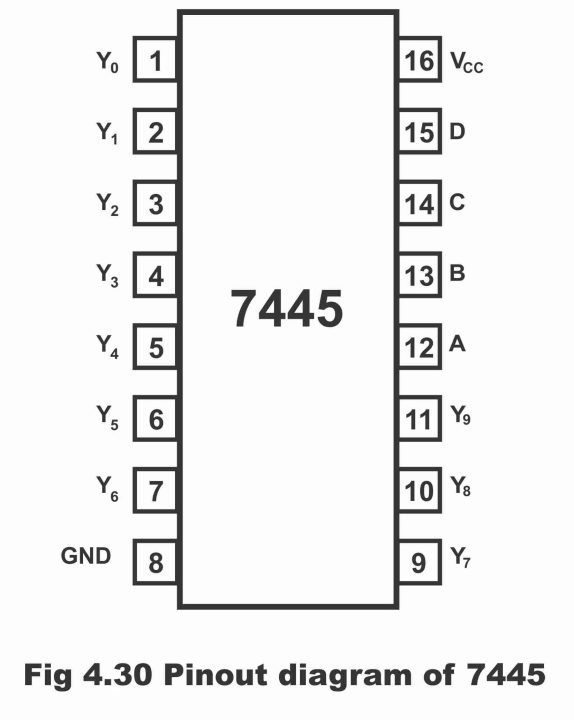
Figure 4.31 – 7445 Truth Table
| No | INPUTS | OUTPUTS | ||||||||||||
| A | B | C | D | Y0 | Y1 | Y2 | Y3 | Y4 | Y5 | Y6 | Y7 | Y8 | Y9 | |
| 0 | L | L | L | L | L | H | H | H | H | H | H | H | H | H |
| 1 | L | L | L | H | H | L | H | H | H | H | H | H | H | H |
| 2 | L | L | H | L | H | H | L | H | H | H | H | H | H | H |
| 3 | L | L | H | H | H | H | H | L | H | H | H | H | H | H |
| 4 | L | H | L | L | H | H | H | H | L | H | H | H | H | H |
| 5 | L | H | L | H | H | H | H | H | H | L | H | H | H | H |
| 6 | L | H | H | L | H | H | H | H | H | H | L | H | H | H |
| 7 | L | H | H | H | H | H | H | H | H | H | H | L | H | H |
| 8 | H | L | L | L | H | H | H | H | H | H | H | H | L | H |
| 9 | H | L | L | H | H | H | H | H | H | H | H | H | H | L |
| H | L | H | L | H | H | H | H | H | H | H | H | H | H | |
| H | L | H | H | H | H | H | H | H | H | H | H | H | H | |
| H | H | L | L | H | H | H | H | H | H | H | H | H | H | |
| H | H | L | H | H | H | H | H | H | H | H | H | H | H | |
| H | H | H | L | H | H | H | H | H | H | H | H | H | H | |
| H | H | H | H | H | H | H | H | H | H | H | H | H | H | |
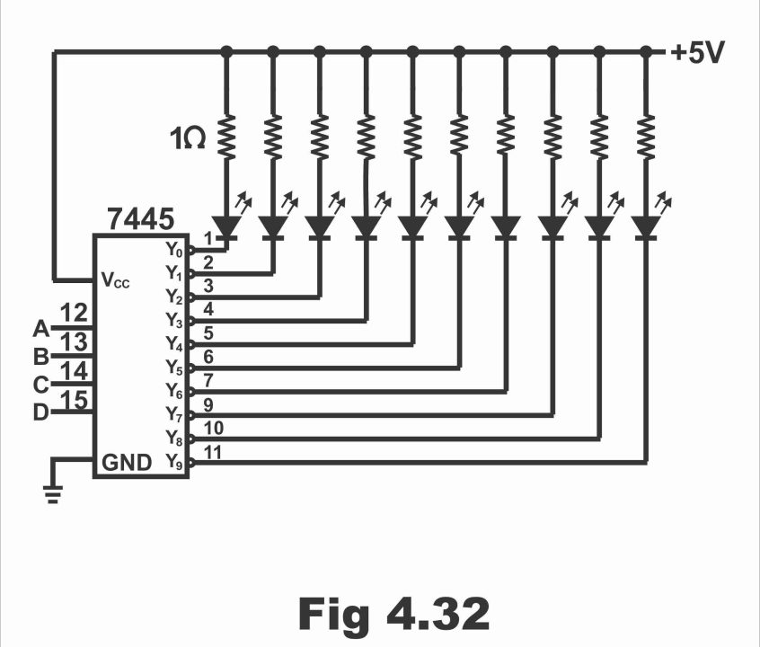
The decoded outputs of a 7445 can also be connected with light emitting diodes (LEDs), as has been depicted via figure 4.32. As activated output of 7445 is low, which means that LED fitted along this gate, which converts a BCD code applied on input to an equivalent decimal number, will not irradiate or illuminate, whereas rest of the LEDs will start to radiate (because outputs of their gates is high). On the contrary, if all LEDs are fitted on a reverse polarity, (i.e. if all LEDs are mounted in a common anode mode), as can be seen via figure, then LEDs will illumine as a result of activated output, whereas remaining LEDs will remain off as usual. In such a situation, truth table will change altogether i.e. on output side of this table, 0 or low will be replaced by 1 or high.
Figure. 4.32
Light Emitting Diode (LED)
A light-emitting diode (LED) is a PN junction or diode, which emits light when it is forward biased. The reason of emission of light lies in the fact that when a LED is forward-biased, free electrons and holes combine together near to this junction (or holes and electrons recombine). As soon as free electrons drop down from their higher energy level to low energy level (i.e. on holes), they emit energy in the form of heat and light. However, if gallium, arsenic and phosphorous etc. is used instead of silicon or germanium for the construction of a PN diode, in such a situation, electrons–emitted energy is achieved in the form of light or photons instead of heat. If the semiconductor material is transparent, it emits light and its junction becomes a light source or light-emitting diode. Remember that colors (e.g. red, green, blue and yellow etc.) of light emitting from a LED depends on the type of semiconductor material (i.e. a manufacturer can design such LEDs by means of using elements such as gallium, arsenic, and phosphorous which emit red, green, yellow, blue, orange, infrared or invisible light). LEDs which produce visible light, are used for the purpose of test instruments, pocket calculators, control panels and for different symbols and readings.
Previous Topic: Demultiplexer or Distributor with circuit diagram and operation
Next Topic: seven segment display truth table and circuit diagram
For electronics and programming-related projects visit my YouTube channel.
Discover more from Electronic Clinic
Subscribe to get the latest posts sent to your email.

good explanation