photodiode Basic Construction and Working
Last Updated on April 17, 2022 by Engr. Shahzada Fahad
Table of Contents
PhotoDiode
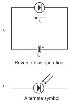
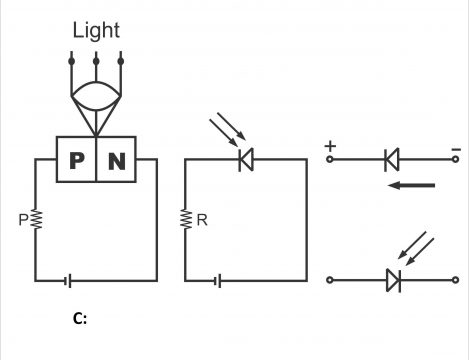
A diode, in which reverse current varies directly in proportion to the quantity of light reflected on it, is called a photodiode. In other words, the photodiode is a PN junction device, that operates in the form of a reverse bias (figure 3.14 a). (Remember, light is a form of energy and according to quantum theory, light consists of small energy packets, which are called photons. Energy found in a photon depends on the frequency of light). There is a small transparent window above the photodiode, light passes through it and collides with the PN junction. In figure (b) symbol of the photodiode has also been shown. They consume little power.
Construction
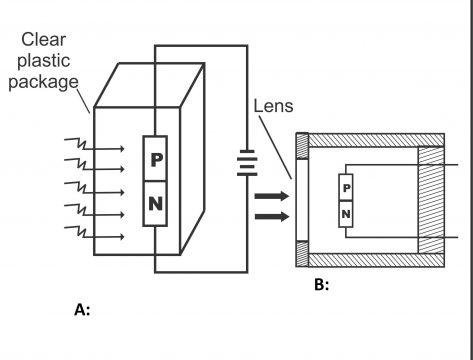
A photodiode is just like a conventional semiconductor diode or a PN junction diode, with the only exception that a lens is mounted above its PN junction in order to focus rays of light. Light reflects on the PN junction passing through this transparent lens. In figure 3.15, the construction of a PN junction photodiode has been given. In other words, a photodiode consists of a PN junction formed as a result of the recombination of P and N types of materials. This PN junction is enclosed in a transparent glass or plastic crust. The entire crust of diode is painted black with the exception of the front part of the PN junction. In this way, rays reach the junction transmitting through the transparent plastic or lens. In figure 3.15 (c), the construction of a photodiode, its biasing, and its symbol have been explained. As is clear from the diagram, a lens has been mounted above the unit, which focuses maximum light reflected on a reverse-biased junction. Remember, an active diameter of a photodiode is about 25 millimeters; however, they are always used in standard pictures for passing maximum light through a built-up window.
photodiode Working
A photodiode normally works in reverse bias mode. We know that when a PN junction is reverse biased, a reverse saturation current passes via the junction, which is generated through holes, electrons, or minority carriers produced as a result of heat. Maximum electrons pairs and holes produce due to an increase in junction temperature, thus minority carriers (or reverse) current also increases. In case a junction is illuminated, exactly the same situation takes place.
In other words, if the PN junction or diode is reverse biased and illuminated, a very small saturation current (I0 or Is) starts flowing through it, which is caused by heat through generating electron- holes pairs (In silicon, the value of (Is)is being measured in nono amperes). The number of these minority carriers depends on the intensity of light reflected on the junction (i.e. reverse saturation current or diode current is about directly proportionate to the intensity of light rays reflected on the junction). When a diode is enclosed in a glass or plastic crust, light illuminates’ the junction and changes the reverse current easily. In case no light rays fall on the reverse bias diode, diode current equals reverse saturation current (I0). Remember, in the absence of light on the junction, the junction’s resistance becomes very high. In case light falls on the junction, minority carriers acquire thermal energy, due to which junction’s resistance subsides and covalent bonds start breaking up in large numbers (or more electron-holes pairs are produced). Resultantly, more current carriers are received and thus reverse current increases. The more the energy of light, the more will be the value of diode current.
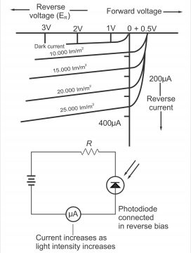
In figure 3.16, the connection of a photodiode and its reverse voltage properties have been illustrated. It clearly indicates that I or IR will increase with an increase in the level of light. Dark light is the light, which reflects on a junction at a time when it is dark or when no light falls on the junction. Reverse current can be changed through a change in the level of illumination or intensity of light reflecting on the junction. Thus diodes’ reverse resistance tends to change. However, remember that no change occurs in reverse current as a result of an increase in reverse voltage. If the value of reverse current is desired to be brought to zero, the diode is forward biased equivalent to the quantity of barrier potential.
Photodiode Uses
A photodiode can power on /off its current in a nanosecond and as such these are the most high-speed detectors. They are used in places, where high switches are required to be powered on/ off at a maximum rate. Some of the uses of photodiodes are as below:
Detection 2. Demodulation 3. Switching 4. High Speed-cum- Need Logistics Circuits 5. Optical Communications Devices 6. Encoders 7. Identification of Some Character 8. Punched Tape & Punched Card Readers 9. Movie Sound Pickup Equipment 10. Photo Electric Release 11. Compact Disk Players or Pickup System of CD players
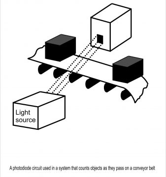
In figure 3.17, common uses of photodiode have been mentioned
Photo-Electric Effect
The emission of electrons from some matter due to the effect of light is called the photoelectric effect. Photo emissive sales, photoconductive cells, photo junction diodes, photovoltaic cells, and photoelectric devices are various forms, which work on the principles of the photoelectric effect.
When a definite light frequency (threshold frequency) reflects on some kind of a metal surface, emission of electrons commences from the metal’s surface. The emission of electrons continues so long as specific frequency light reflects on the metal surface. Electrons emitted from some metals’ surfaces due to the effect of light are called photoelectrons and this phenomenon of electrons emission from a metal’s surface as a result of light is called photoelectric emission. This effect was first observed by Hermes. He observed that when ultra-violet rays fall on negative electrodes, a brisk spark produces between the two electrodes. After a lot of research, the following two laws of photon electric emission were described.
The number of electrons emitted in a second from some sensitive surface is directly proportional to the quantity of light flex on the surface.
The maximum kinetic energy of electrons emitted from some photo-sensitive surface remains independent from the quantity of high flex, however, its relation to flex (light) frequency is linear or directly proportionate.
When photo energy collides with some metal surface, the surface absorbs this energy. Photon energy is as under:
F= bf Joules
Here “f” means frequency, and “b” is a Plank’s constant, the value of which is equal to 6.625 x 10¹⁴ joules second. Remember that, the wavelength is inversely proportional to Lambda frequency and photon energy is directly proportionate to its frequency. A photon also has a mass and momentum; however, it does not have electric charges on it.
The emission of electrons, resulting from the collision of light energy with some metal’s surface, is called photoelectric emission, which was discovered by a famous British scientist Joseph J. Thomson in 1897.
According to Plank’s light theory, light is a form of energy consisting of small packets, called photons. Thus, every photon has energy. When light collides with some metal surface, due to extreme energy produced, the valence electrons of the metal surface move to the conduction band from the valence band(in other words, valence electrons on the metal surface, change their energy level as a result of the acquisition of energy from light and thus, valence electrons change their place)
For example, if ultraviolet rays are reflected on a negatively charged zinc plate, electron emission starts from its surface. Apart from zinc, the objective can also be achieved through other metals e.g. rubidium, sodium, potassium, lithium, cesium, etc. Remember, metal with the lowest work function (energy required for emission of an electron from metal, is called work function of metal) is most suitable for photoelectric emission e.g. cesium. The work function of this metal is 1.9 electrons volt. Copper’s work function is 4.3 electrons volt (eV). Therefore, the emission of electrons from copper with one photon energy is not possible.
The photoelectric effect can also be elucidated with the help of the following experiment.
Photodiode Experiment
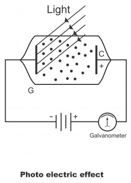
For example, there is a glass tube, which is completely devoid of air i.e. it is air-tight. The glass tube consists of a metal plate P and an electrode C. Plate P has been connected with negative, whereas electrode C with positive terminals of the battery. When light reflects on plate P, the emission of electrons starts through it (i.e. metal plate operates as an emitter). Electrode C attracts emitted electrons towards it (i.e. electrode C works as a collector). A galvanometer has also been fitted in the series circuit (figure 3.18). The galvanometer is a meter, which measures very small quantities of current and voltage.
When light casts on plate P, electrons emit from its surface. In other words, due to being inversely charged, electrode C attracts plate P electrons towards it. As there is a negative charge on electrons and plate P also being connected with negative terminal of battery, therefore, plate P repels electrons emitted from the metal surface towards electrode C. Due to the flow of electrons towards electrode C, the galvanometer fitted in the circuit, indicates surface current. The flow of current in the circuit continues so long as light falls on plate P. As soon as the light is cut off (due to turning the switch off), the galvanometer reading also becomes zero, and thus flow of electrons in the tube, also comes to an end, as circuit current becomes zero.
The following information has been gathered in light of the aforementioned experiment.
- Electrons do not emit so long as the light does not reflect on metals’ surface
- If the light frequency colliding with the surface is less than the threshold frequency, electrons emission from metals’ surface cannot occur. The minimum frequency of some specific light wavelength, on which a metal starts emitting electrons, is called threshold frequency. It is denoted by f0, whereas the related wavelength of threshold frequency, is called threshold wavelength (λ0). Its value is 2.744x 10⁻⁷ Thus, the following relationship is found between threshold frequency and threshold wavelength.
F0= c/ λ= 3×10⁸/2.744x 10-7 = 109x 1015 c/s
- The photoelectric threshold frequency depends on the nature of metal
- Increasing frequency above the threshold level, the energy of photoelectrons increases
- Photoelectron energy does not depend on the intensity of light, it rather depends on the frequency of light
- Electrons emitted from the plate are directly proportional to the intensity of light
- The emission of photoelectrons stops immediately upon disruption of light
Specific constants’ tables of photoelectric emitters have been given in table.
| Substances | Work Function, Diode | Threshold wavelength Angstrom units |
| Cesium oxide – silver
Sodium Potassium Rubidium Lithium |
1.8
2.5 1.9-2.46 1.8-2.2 2.1-2.9 |
11.000
7.000 6.000 6.800 5.300
|
PhotoTube
A phototube is a practical shape of photoelectric effect which has been illustrated in the diagram 3.19
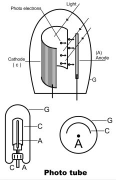
A phototube is broadly used as a photoelectric device. It is composed of steel or nickel half-cylinder and a narrow thin metal-made rod. There is a layer of Cesium or Potassium on the interior surface of the half-cylinder. Sometimes, a half-cylinder is manufactured by putting a thin cesium layer over emissive material silver oxide and sometimes through a thin cesium layer above antimony on the plate. The cylinder works as a cathode, whereas a narrow metal rod (about 1 mm in size), fitted parallel to the center of the cylinder, works as an anode. The cathode and anode, both are enclosed in an air-tight glass tube (G). For connecting with the circuit, the anode and cathode both are fitted on a Bakelitebase through prongs and pins. Remember, a phototube is also called a photoemissive cell.
Applications
Under an automatic system, phototubes are used as door openers, on/off cinema projector circuits, counting or sorting operations, inspection, fire alarms, photoelectric, and photometry.
Photo Conductive Effect
When light reflects on some of the metals, their conductivity (capacity to pass on current) changes e.g. cadmium sulfide, solenoid, selenium, etc.). In absence of light, the resistance of these types of metals is very high, whereas their conductivity is low. Remember, that resistance and conductance are mutually inversely related. Such materials are called photoconductive materials. The change in conductivity due to the reflection of light on any material is called photoconductivity. Change in electrical conductivity under photoelectric effect during the reflection of light on some metal or semiconductor, is called photoconductive effect or a photoelectric effect, due to which conductivity of certain semiconductor material changes, is called photoconductivity effect. Items, the resistance of which depends on light, are called resistors or photoconductors. The photoconductive effect is used in photoconductive cells, TV, camera, tubes, phototransistors, etc.
Photo Conductive Cell
A photoconductive cell or photoresistor is a semiconductor device, comprising two terminals and the terminal resistance of which change due to the reflection of light on it. In other words, instruments, the conductance of which change due to the quantity of light being reflected on them (because their dark resistance is high) are called photoconductive cells or photoresistors. As a special term, they are also known as LDR (Light Dependent Resistors)
Working Method
When the light of some specific frequency and suitable energy reflects on photoconductive materials (e.g. cadmium, sulfide, cadmium solenoid, lead solenoid, thallium sulfide, cadmium Neoloride) its surface electrons isolate themselves from covalent bond through absorbing light energy (for free movement of an electron, its independence from the influence of a parent atom is essential. This task is taken from light, as electrons change energy levels through absorbing energy from light. Thus, they become independent from the effect of the ambit of its atom). Thus, material resistance gets lower due to the formation of electron-hole pairs, or charge carriers on the surface of photo-sensitive material. Remember, the larger the number of electron-hole pairs, the higher will be the current.
Construction
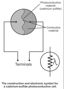
In figure 3.20, the construction of a photoconductive cell and its symbol has been given.
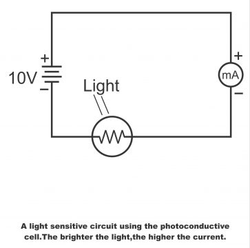
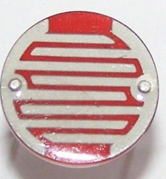
Photoconductive material (cadmium sulfide) has been mounted on a ceramic made insulation disk. There is also a layer of conductive material overlapping the insulating disk. When light falls on the material, its conductivity increases or its resistance declines. It controls the current in a cell circuit and is used for operating meters and relays directly. In figure 3.21, a photoconductive cell has been displayed fitted on the series circuit with a current meter and power source. As the intensity of light increases, the current also increases.
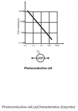
In figure 3.22, cell properties have been displayed. From the figure, it is evident that cell resistance is even greater than 100KΩin the absence of light. This is called dark resistance. When light falls on the cell, its resistance gets reduced to a few 100 ohms. As compared to other cells, this particular cell turns out to be more sensitive. It is low in price and its dark to light resistance is also quite high. A particular cadmium sulfide photoconductive cell has been illustrated in diagram 3.23 (a).
Uses
Due to dependence on light, these cells are commonly used in industries for various tasks e.g. counting and sorting, fire and burglar alarm system, automatic door openers, safety warning systems, increasing computer information, ships and aircraft detection, light meters, on-off switches, relay controls, voltage regulator and automatic parking lights, etc.
For electronics and programming-related projects visit my YouTube channel.
Previous article: Series and Shunt Voltage Regulation and Next article: Photovoltaic Effect
Discover more from Electronic Clinic
Subscribe to get the latest posts sent to your email.
