Series Voltage Regulator and Shunt Voltage Regulator
Last Updated on April 17, 2022 by Engr. Shahzada Fahad
Table of Contents
Description:
Series Voltage Regulator and Shunt Voltages Regulator- in this article, we will discuss series and shunt voltage regulators in detail.
Voltage Regulation
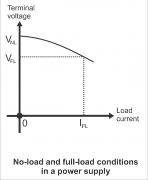
An exemplary power supply always has constant voltages on output terminals, irrespective of the values of current received (or within its rated current capacity, whatever the value of load it is connected with). However, output voltages, in a practical power supply change with the value of its load current (usually with an increase in load current, voltages of power supply decrease or drop). Specifications of a power supply also contain its full load current ratings (IFL), which is the maximum current received through the supply. When full load current is being achieved, at that point, terminal voltages of the power supply are called full load voltages (VFL). No-load voltages (VNL) are open circuit terminal voltages i.e. when no current is being received from the supply (zero current), terminal voltages of the power supply at that time are called no-load voltages. In figure 1, no-load and full load conditions of power supply have been illustrated.
Measurement of efficiency of a power supply, through which it could be ascertained, how better a power supply is, enables a power supply to keep it on a constant voltage between no load and full load conditions. Its percent voltage is called regulation. (Percent voltage regulation value of a correct power supply is zero) i.e.
Voltage Regulators
A voltage regulator is a device or set of devices designed in such a manner that it maintains the output voltage of a power supply constant to the maximum possible extent. It is also called a closed-loop control system because it provides feedback via examination of output voltages. It compensates for every tendency of output voltages and increases or decreases supply voltage automatically according to requirement. Thus, the objective of a regulator is to eliminate any changes in output voltage (which may result from a load change, input voltage changes, or temperature change). There are two types of voltage regulators.
- Series Voltage Regulator
- Shunt Voltage Regulator
Series Voltage Regulator
A regulator, the control element (normally a transistor) which is mounted within a series of input voltage and output voltage, is known as a series voltage regulator.
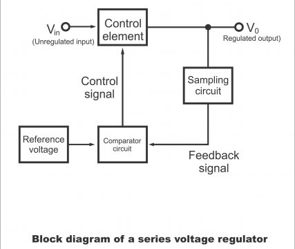
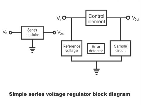
In figure 2, a functional block diagram of a series type regulator has been shown. A functional diagram works as a useful model so that the principles of a series regulator model could easily be understood. Output, senses variations in a simple circuit, output voltage, error detector compares simple voltage with a reference voltage, and thus provides signals to control element for maintaining a constant output voltage. Along with a filter capacitor, unregulated DC input supplied through a rectifier (shown as Vin in the diagram), is passed on to the control element mounted in the regulator, through the output of which, regulated output voltages (V0) are produced. Control Element is a device, by means of which constant output voltages are acquired by adjusting its operating state according to needs. As a control element is being fixed in series between (V in) and (V0), therefore, such type of regulator is also called series type voltage regulator. A sampling circuit produces feedback proportionate to the output voltage (V0). These feedbacks are received by the comparator circuit in the form of a signal, which through mutual comparison of the reference signal and feedback signal provides its output to the control element in the shape of the control signal. This control signal adjusts the operating state of a control element.
For example, if V0 reduces due to an increase in load, the comparator produces such an output (or provides such a control signal), due to which control element increases (V0). In other words, Vo increases automatically until the comparator circuit, sensing fresh variations between the feedback signal and reference voltage, starts providing a new control signal to the control element. Exactly the same way, the comparator circuit passes such a control signal to the control element as a result of an increase in V0 (due to reduction in load), as a result of which V0 decreases. For further clarification, a block diagram of a series voltage regulator has been shown in figure 3
Transistor Series Voltage Regulator
In figure 4, a simple series type voltage regulator consisting of a transistor has been demonstrated. Here, the NPN resistor functions as a control element, which is frequently called a pass transistor, because through conducting, it passes the entire load current through the regulator. Normally, it is a power transistor mounted on a heat sink. Zener diode provides voltage reference. As the entire output voltage (V0) is used for feedback in such types of circuits, therefore, it does not contain any sampling circuit.
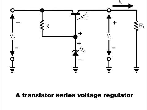
As is evident from the diagram, the Zener diode is reverse bias, and reverse current is supplied to it through resistance R. Although, (Vin) is unregulated, its values are kept maximum to a reasonable extent and the value of R kept low to a suitable extent so that Zener could be retained in its reverse breakdown region. Thus, Vz remains constant despite a change in input voltage, (Vz) remains unchanged. If Kirchhoff law is applied around the output loop, we get the following equation
VBE= Vz– V0
According to the equation, if (Vz) is constant, a change in (VBF) occurs due to any variation in (V0). For example, if V0 is reduced, (VBE) must necessarily increase (as Vz are constant). Similarly, if V0 increases, (VBE) must decrease.
When V0 is reduced, (VBE) tends to increase, due to which conduction of NPN transistor also increases. Thus, load current increases, due to which an increase occurs in V0 (because of V0= IL RL). On contrary, when V0 increase, (VBE) decreases, due to which transistor’s conduction also reduces (i.e. low current passes through it) thus load current, reduces, and resultantly (V0) also decreases.
Shunt Voltage Regulator
A regulator, the control element of which is parallel to the load, is known as a shunt regulator (figure 5). For further elucidation, a functional block diagram of a shunt type regulator in figure 6 has been revealed. Components in the block diagram perform exactly the same functions which components in a series regulator use to perform. However, it has to be remembered that the control element in a shunt voltage regulator is parallel to the load, which it is called a shunt regulator. The control element, in case of changes in load current (IL) maintains a constant load voltage on load, by passing a low or high shunt current (I SB) from within it.
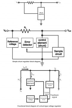
If the control element is considered a variable resistance as per the diagram, the process of the control element becomes easy to understand. For example, in case of a decrease in load voltage, the resistance of the control element increases automatically, thus small current flows towards the control element, and load voltages increase. Inversely, if load voltages are increased, the resistance of the control element gets low, thus load voltage decrease due to the passing of more current through the control element.
In other words, source resistance (Rs) on the input or unregulated side of the diagram; assumes the shape of a voltage divider, due to parallel mounting of the control element and (RL) (i.e. it operates as a voltage divider). Thus, when the resistance of a control element increases, the resistance of the parallel combination increases, and load voltage also increase as a consequence of voltage divider action.
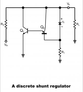
Discrete Shunt Voltage Regulator
In figure 6, an individual or discreet (composed of isolated or separate parts) shunt voltage regulator has been exposed, in which transistor Q1 functions as a shunt control element. As Zener voltages (Vz) are constant, therefore any changes in output voltage cause a proportionate change in voltage parallel to (R L). Thus, if (V0) decreases, voltage parallel to (RL) also decreases. As voltages parallel to (RL) are also base voltages of Q2, therefore, base voltages of Q2 also decline. Thus, conduction of Q2 decreases due to which base current of Q1 also declines. Thus, conduction of Q1 also diminishes due to a low base current and it thus, shunts a small current through the load (a small current pass through it), as a result, load voltage increases. Inversely, conduction of Q1 and Q2 increases due to an increase in V0 thus, a very low current passes towards the load (in other words, a higher current passes through Q1 as a result of an increase in its conduction), resultantly (V0) automatically decrease.
For electronics and programming-related projects visit my YouTube channel.
Previous article: Zener Diodes and Next article: PhotoDiode Construction and Working
Discover more from Electronic Clinic
Subscribe to get the latest posts sent to your email.


Great post! I found the comparison between series voltage regulators and shunt voltage regulators very informative. It’s interesting to see how each type has its own advantages depending on the application. Looking forward to more insights on practical implementations!
Great post! I found the comparison between series voltage regulators and shunt voltage regulators really insightful. It clarified some concepts I was struggling with. Thanks for breaking it down so well!
Great insights on the differences between series voltage regulators and shunt voltage regulators! It’s fascinating to see how each type has its unique applications and advantages. I particularly liked the detailed examples you provided; they really clarified the concepts. Looking forward to more posts like this!
This post was incredibly informative! I appreciated the clear comparison between series voltage regulators and shunt voltage regulators. The diagrams helped solidify my understanding of how each type functions in different applications. Thank you for breaking down these concepts so well!