Zener Diodes Basic Operation and Equations
Last Updated on April 8, 2022 by Engr. Shahzada Fahad
Table of Contents
Zener Diodes
It is a heavily doped reversed bias PN junction device, manufactured either from silicon or germanium and it operates in the breakdown region (or at Zener point) where the excessive current is confined via external resistance as well as internal waste power within a diode. Silicon is preferred over germanium due to its high current and high-temperature properties. In other words, the Zener diode is a diode, which normally functions in a breakdown region (remember that due to possible disadvantages of a rectifier diode, it is never used intentionally in the breakdown region). The breakdown voltage of a Zener diode is very carefully set by controlling the doping level. Zener diode is mostly applied in voltage regulator circuits. In such circuits, DC load voltage almost remains constant despite variations in line voltage or load resistance.
Zener effect and avalanche effect both exist at the time of breakdown of a diode. Though either the first or second effect turns more dominant, the dominance of any of these two effects depends upon the value of reverse voltage. In the case of reverse voltage less than 5 volts, Zener effects become predominant, while avalanche effect takes dominance when voltage is above 6 volts. Both effects lie between 5 and 6 volts. Cautiously, the first is called Zener diode and the second one is known as avalanche diode; however, together both are commonly known as Zener diodes.
Zener breakdown occurs when a strong electric field sets up in the depletion region and via the breaking of covalent bonds as a consequence of this field due to low reverse voltage. Thus, a very large number of electrons and holes are formed, which generate reverse saturation current (now known as Zener current Iz), the value of which is controlled or restricted through external resistance in the circuit. Avalanche breakdown occurs on very high reverse voltages when thermally generated electrons form more carriers through collision resulting from acquiring suitable energy.
Basic Theory Zener Diode:
We know that when a PN junction is reversed bias, a point comes where junction breakdowns and reverse current also increases at a very fast pace, the value of which is limited through fixing an outer resistance in a series of junctions. This critical value of voltage (on which this situation takes place) is called breakdown voltage (VBR). Once breakdown has occurred current value witnesses a major increase due to an additional increase in voltage. At this point junction itself offers nearly zero resistance.
Breakdown voltage depends on the breadth of the depletion region. However, breadth itself depends on the doping level. Due to an increase in reverse voltage two mechanisms are responsible for a breakdown, or in other words, a breakdown takes place due to the following two effects.
Zener Breakdown
This kind of breakdown occurs in junctions that are quite heavily doped and their depletion layers are narrow. Breakdown voltage forms a strong electric field (108 v/m) parallel to this narrow layer. Covalent bonds break up due to a strong field and electron-hole pairs are formed (in other words, this strong field pulls valence electrons out of their respective shells). Now if a further small increase in the reverse voltage is applied, large current carriers are formed consequently. This is the reason, that junction resistance in a breakdown region is very low and a large reverse current generates. As valence electrons are isolated through an electric field under the Zener effect, it is also sometimes known as high field emission.
Avalanche Breakdown
This kind of breakdown occurs in junctions that are lightly doped and its depletion layers are wide, while its electronic field is not so strong that a Zener breakdown could be triggered. However, minority carriers moving in the field, collide with semiconductor atoms in the depletion region. As a result of a collision with valance electrons, covalent bonds break down and electron hole-pairs are formed. The electric field further intensifies the speed of these newly formed charged carriers, due to which further collisions occur, thus more charge carriers are produced. In this way, a spate of charge carriers happens, which is called an avalanche. Due to this, the junction’s reverse resistance becomes low. In other words, when the diode is reverse biased, minority carriers generate little reverse current at the breakdown point. When diodes’ reverse voltage is enhanced to an extent that its value exceeds the breakdown voltage, the energy of minority carriers gets so high, that valence electrons isolate from their normal orbits. These isolated electrons become free electrons and other valance electrons also start forming free electrons through isolation from their orbits. Thus, due to an avalanche of free electrons, a large reverse current generates.
The condition of the above-mentioned breakdowns has been illustrated in figure1
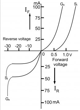
V/I Current Characteristics
Voltage-current characteristics of a Zener diode have been illustrated via figure2. Its forward characteristics are straightforward just like an ordinary forward bias junction (figure1). However, salient points of its reverse characteristics are as follows:
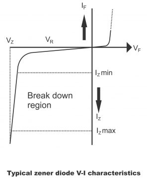
Vz= Zener breakdown voltage
Iz.min= minimum current to sustain a breakdown
Iz.max= maximum Zener current limited by maximum power dissipation
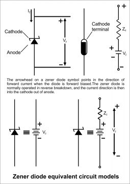
Due to a diodes’ resistance (called Zener dynamic impedance, its value is almost equal to nothing with respect to the value of outer resistance in the circuit), the reverse characteristics of a Zener diode are not at all vertical. However, we ignore it and assume that its characteristics are vertical. In other words, we treat Zener as an ideal diode with no changes in its voltages due to a breakdown. It means that Vz remains constant despite an increase in the values of Iz. In figure3 (a), the shape of a Zener diode, in figure (b) low power diode, and in figure (c) its equivalent circuit has been shown. The symbol of a Zener diode shown in figure (a) just resembles a normal diode, with only the exception that the ends of two lines separating cathodes are curved. It can be observed that the symbol of a Zener diodes’ cathode is just like the English alphabet “Z”. In figure3, an ideal and practical Zener diode has been illustrated along with its equivalent circuit, in which it looks like a V volt battery.
Zener Biasing
For working efficiently with a Zener diode on any circuit, it is necessary that
- It should be reverse biased
- It should have more voltage compared to Zener breakdown voltage (Vz)
- It should be fixed on such a circuit, which passes less current compared to I z-max
Working of Zener Diode;
When a Zener diode is forward biased, due to a very low forward resistance it starts conducting at 0.7 volt (0.3 volts in the case of germanium) just like a silicon diode and its forward currents increase too rapidly. When it is reverse biased, very small leakage or reverse current flows through the leakage region (the region between zero and breakdown) due to large reverse resistance. When it’s reverse biasing is further increased, a point is reached where (or a specific value of reverse voltage) diode break downs, by means of which reverse current increases very briskly. This current is normally confined via inserting resistance in a series of Zener diodes. This increase in reverse current is almost vertical (as evident from V/I characteristics). Remember, the voltage in the breakdown region is nearly constant and its value almost equals Vz.
Rating of Zener Diode:
The voltage rating of a Zener diode is described with respect to Zener voltage. Normally, various Zener diodes of Zener voltages are available. Zener diodes with Zener voltages or breakdown voltages ranging between 1.8 V to 200 V, are common, whereas the limit of permissible variations in its ratings is 5-10 percent and sometimes 20 percent. However, its Zener voltages depend on doping level and temperature.
Consumption power of a Zener diode equals the product of its voltage and current i.e.
Pz = Vz. Iz
As long as the ratio of power rating of a Zener diode is less than Pz, it operates in the breakdown region without any damage or becoming ineffectual. The power ratings of commercially available Zener diodes normally range between 50w to 150mw. Normally on a datasheet, apart from breakdown voltage (Vz), maximum current is also supplied to a Zener diode, through which a Zener diode can pass without its power ratings being increased. On datasheets, the maximum consumed power of these Zener diodes at a specific maximum temperature, is also being given, which can be too high. Zener diode normally resembles just another diode; however, it is identified from its IN number e.g. IN750 or IN4000. The power of IN 750 is 10 watts whereas IN4000 is a high-powered diode.
In table 3.1, ratings of Zener diodes or voltage regulator diodes ranging from IN746 to IN 759, have been illustrated.
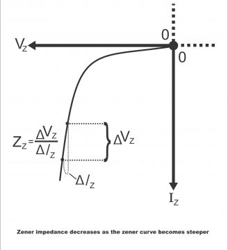
Zener Diode Impedance
Another important parameter of the Zener diode is Zener impedance (Zz). Zener impedance is basically a Zener diodes’ dynamic resistance or impedance(just like the dynamic resistance of an ordinary PN diode). The inverse slope of a Zener curve is called Zener impedance. The slope of a Zener curve (V/I) is ∆I/∆V as impedance equals ∆V/∆I therefore, Zener impedance, is inverse of slope)
Zz= ∆Vz / ∆Iz =Change in zener voltage/ Change in zener current
Zener impedance reduces due to an increase in Zener current and the Zener curve assumes the shape of a straight slope (figure4). As Zz represents a sloped curve, therefore, its lowest value is normally more significant, particularly where a very low change in voltage via a maximum change in current is required. However, it is an important property of a Zener diode while working in the breakdown region.
Uses of Zener Diode:
Zener diodes are extensively used in transistor circuitry. Some of these uses are as below:
- For voltage regulation
- As peak clippers or voltage limiters
- Avoiding high voltages for meter protection
- For reshaping a waveform
- As fixed reference voltage for the purpose of biasing and comparison in any network and for calibrating volt
Uses of a Zener Diode as a Voltage Regulator
Measuring the capacity of a constant voltage supply in spite of variations either in input voltage or load current is known as voltage regulation of current. We know that the most important function of a voltage regulator is a constant supply of output despite large variations in load current and as a Zener diode is applied in some voltage regulators, it performs this function as a regulator in an excellent manner. Therefore, the Zener diode is occasionally defined as a diode, which is used as a voltage regulator.
Remember, an ordinary diode cannot function as a Zener diode, because ordinary diodes operate in a forwarding direction, whereas a Zener diode is mounted on a circuit for working in the reverse direction. As Zener diode operates in the breakdown region, source voltage Vin must always exceed Zener breakdown voltage (Vz)
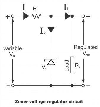
In figure5, a simple Zener voltage regulator circuit has been shown, in which Vin are DC voltages, variations in which have to be regulated. Zener diode is mounted parallel to Vin. It conducts when the voltage value parallel to the diode is greater compared to Vz and a large current start passing through the series resistance Rs. Load resistance RL parallel to which constant voltage Vout is required is mounted parallel to the diode. Total current (I) passing through Rs equals a total of diode current (Iz) and load current (IL).
I= Iz+ IL
Remember, all the time and under any conditions, output voltage (Vout) must always equal Zener voltage Vz i.e. Vout= Vz
Therefore, Vin= IRs+Vout= IRs+Vz
(1). In the first situation, suppose that value of R is fixed or constant, whereas the value of supply voltage (Vin) has increased a little. As per ohm law, circuit current tends to increase with an increase in supply voltage. Thus, an increase in (Vin) will also increase the drop existing parallel to the series resistance (Rs). Consequently, (Vout) remains constant. On the contrary, if supply voltage (Vin) is decreased, the low current passing through the diode and voltage drop parallel to (Rs) also decrease, due to which (Vout) remains constant again. Thus, when (Vin) changes, I and Rs drop also change, and (Vout) or (Vz) remain unchanged.
(2). In other situations, suppose (Vin) is fixed, however current passing through the Zener diode (Iz) varies. When load current (IL) increases, diode current (Iz) decreases. In this way, (I) and (Rs) remain fixed, and (Vout) also does not change at all (i.e. there is no impact on (Vout). If (IL) reduces, (Rs) will increase, so that (I) and (Rs) drop remain unchanged. Therefore, (V out) does not change in spite of a decrease in (IL), because
Vout= Vin– IRs= Vin– (Iz+ IL) Rs
However, remember that value of (Rs) is determined as under:
Rs= Vin– Vout/ Iz+ IL = Vin– Vout/ I
When value of diode current is maximum, value of (IL) becomes zero. i.e.
Rs= Vin – Vout/ Iz. max
Example
Suppose the value of (Vin) is 30-volt, the value of (Vz) is 12 volt and the value of series resistance is 1.8 kn. As input voltage exceeds Zener voltage, therefore, Zener diode starts working in the breakdown region and supplies 12-volt output voltage. However, the value of Zener current or the current passing through series resistance is determined as follows.
I= Vin– Vz/Rs= 30V-12 V/1.8KΩ= 10mA
Now, if the value of input voltage is increased from 30 to 48, the value of Zener current will be as under.
I= 48V-12 V/ 1.8 KΩ = 20mA
As the breakdown region is almost vertical, therefore, despite variations in input voltage (30 to 48 volts) and in values of operating current (10mA to 20mA), output voltage parallel to the Zener diode, almost remains constant i.e. 12 volts.
For electronics and programming-related projects visit my YouTube channel.
Previous article: Diode as a Switch and Next article: Voltage Regulation
Discover more from Electronic Clinic
Subscribe to get the latest posts sent to your email.