Unijunction Transistor UJT, Construction, Working and Solid State Device
Last Updated on June 19, 2022 by Engr. Shahzada Fahad
Table of Contents
Unijunction Transistor UJT, Description:
As the name implies, this transistor consists of just a single junction. In other words, a transistor in which there is only one junction is called a unijunction transistor. Basically, it is a silicone diode having three terminals. It is different from an ordinary diode in the sense that it has three leads and from a FET it is different in the sense that it does not possess any amplifying capacity (that’s an ordinary diode has two leads whereas a unijunction transistor has three leads. Further, FET has an amplifying quality, whereas it does not have this quality). However, it has the capability of controlling high ac power via a feeble signal. As a result of its negative resistance characteristics, it is also used in timing circuits as an over oscillator (when the input voltage reaches a certain level, UJT’s input resistance dwindles very quickly. This effect is called negative resistance characteristics). Remember that a unijunction transistor (UJT) always operates as a switch similar to a four-layer diode.
Construction Of Unijunction Transistor:
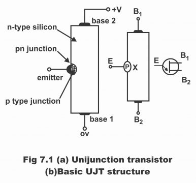
A Unijunction transistor is a single junction comprising three terminals which consist of a lightly doped N-type silicone bar, on both ends of which ohmic contacts are made. Both these contacts are called Base 1 (B1) and base 2 (B2). A small P region exists on one side of the silicone bar, which is quite heavily doped. Remember that this P region manufactured from P-type material is closer to B2 as compared to B1. Thus, the PN junction is formed via penetrating a P-type region into an N-type bar. This P region is an emitter of UJT, in which the number of holes is large. In figure 7.1, the construction of a particular UJT has been elucidated. It can clearly be seen in the figure that three terminals exist on UJT, one of which is an emitter (E), and the other two are based terminals (B1 and B2), which are fitted alternately up and down on the silicone bar.
Figure 7.1 (a). Unijunction transistor (b). Basic UJT structure
Inter-base Resistance
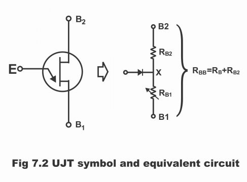
Inter-base resistance is denoted by RBB. It is the resistance between B1 and B2. That’s if the emitter terminal is turned open, it is the total resistance found between one end to the other end of the silicone bar (in other, total resistance between B1 and B2 is called inter-base resistance). Its value ranges usually between 4Ω-10Ω and this resistance can easily be measured via an ohmmeter by turning the emitter terminals open. RBB is basically the total resistance of an N-type bar, thus this inter-base resistance can be converted into two resistances. Resistance from B1 to emitter is called B1, while resistance present from B2 to emitter is called B2. As the emitter is nearer to B2, therefore the value of B2 is higher as compared to B1.
Equivalent Circuit
The operation of a UJT can be elaborated with the help of its equivalent circuit in a better way. Unijunction transistor UJT symbol and its equivalent circuit have been displayed in figure 7.2. The arrow sign in the symbol denotes emitter. Emitter leg is located on an angle at vertical or base (that’s the arrow sign reflecting emitter is slightly curled) and when UJT is in conduction or operational mode, this arrow sign shows the conventional flow of current (that’s the arrow sign represents the flow of holes instead of electrons). The diode sign shown in the UJT equivalent circuit represents the PN junction between the emitter and base bar (point X). The arrow sign above RB1 reflects that it is a variable resistance, because its value changes inversely to I1, and during normal operation, its specific range may be 4Ω-10Ω. Through UJT’s equivalent circuit, the value of RBB can also be reflected.
Figure 7.2 unijunction transistor UJT symbol and equivalent circuit
Intrinsic Stand-off Ratio
The mutual ratio between RB1 and RBB is called the intrinsic stand-off ratio, which is denoted by eta (ŋ). That’s
ƞ= RB1/ RBB
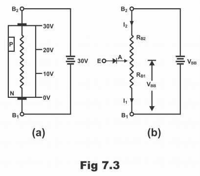
If a 30V battery is fitted parallel to B1B2 by opening the emitter (or ignoring the diode momentarily), as can be seen in the figure 7.3 voltages from B2 towards B1 start reducing step by step (in other words less voltages step by step are found at different points parallel to inter-base resistance RBB). In figure (b), it is evident that the emitter operates as a voltage divider tape on fixed resistance RBB.
When the emitter is open, I1=I2
Value of inter-base current can be determined via ohm law as below:
I1=I2=VRB/RBB
For instance, if the value of VBB is 30 while RBB’s 15Ω, the value of inter-base current will be as follows:
I1=I2=30/15=2mA
It should be remembered that some part of VBB drops parallel to RB2 and some of its part parallel to RB1. Now we determine voltage (denoted by VA) drop parallel to RB1. For this purpose, we use the voltage dividers’ formula, which is as under.
VA=RB1/RB1+RB2 x VBB = RB1/RBB x VBB
Voltage division factor RB1/RB1+RB2 is represented by a unique symbol ƞ (Greek word eta) and it is an internal voltage divider ratio in a UJT, which is known as the intrinsic stand-off ratio. The value of ŋ is usually less than unity (i.e. 0.5-0.85). Thus,
ŋ=RB1/RB1+RB2 VA= ƞ VBB
If VBB=30V, and ƞ=0.6, the potential of point A with respect to B1 will be 18 volt (that’s 0.6×30=18) and the remaining 12 volts drop parallel to RB2.
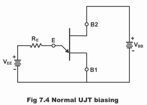
Figure 7.4 Normal UJT Unijunction transistor Biasing
Biasing
i). When the emitter diode is reverse biased, very small emitter current flows. Under such a situation, RB1 remains at its normal high value (usually 4Ω). This is off the state of UJT.
ii). When the emitter diode is forward biased, RB1‘s value decreases. Thus, total resistance between E and B1 gets very low. As a result, the flow of the emitter current starts immediately. This is on state of unijunction transistor UJT.
In order to operate a UJT, both terminals B2 and E are forward biased with respect to B1 as described in figure 7.4. B1 always acts as a reference terminal of B1 and measurement of all voltages is done with regard to B1. VBB source is usually fixed and it provides voltages consistently from B2 to B1. VEE source is normally a variable voltage source and it is called the input of the circuit.
Working or Operation of Unijunction Transistor:
When the VBB switch is turned on, (that’s when fixed dc voltages are provided parallel to B2 and B1) and the variable source provided between emitter and B1 is set to zero, the N-type silicone bar acts just like a uniform resistance bar (the average resistance of both its terminals is from 1500-10000 ohms). Thus, potential VBB is uniformly distributed across parallel to the entire bar and the junction becomes reverse biased. The flow of reverse leakage current through junction starts as a result of it getting reversely biased. This has been illustrated by the curve formed behind point zero or towards its right.
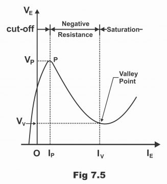
If emitter potential VEE is increased gradually, reverse bias gets less due to which reverse leakage current also becomes less. When emitter voltages turn reverse bias completely neutral, the value of reverse current at that time becomes zero.
Making further increases in emitter voltages, the junction becomes forward bias. When emitter voltages exceed beyond junction barrier voltages (VB), (remember that the value of VB for silicone is 0.7 volts), the emitter current rises very quickly. As a result, a large quantity of current starts flowing through the middle region of junction and B1. Large numbers of holes enter on the lower section of the bar; thus, the resistance of this section dwindles to a very great extent. This brings about a sharp increase in emitter current. This value of emitter voltage is called peak point voltage, which has been denoted by VP in the figure. When VE = VP, emitter peak current IP, flows towards ground or B1 via RB1. In such a situation, UJT is termed as ON or it is said that a unijunction transistor UJT has fired. The number of charge carriers in RB1 increases by means of the flow of IE via RB1, due to which its resistance lowers. As eta (ƞ) depends on RB1, therefore its value is also low.
In this characteristic region, above which P has been engrossed, the device fires, and emitter current transmit through it in a huge quantity. Due to the transmission of high emitter current, large voltage drops occur parallel to RE, which results in lower VE (figure 7.6). It becomes clear that current passing through an emitter increases after the device has been fired, however, a reduction occurs in voltages being found on the emitter. Due to this, a negative resistance sets up which continues until emitter voltages reach their lowest value (i.e. negative resistance region survives continuously so long as the emitter voltage value does not reach its minimum). This minimum value of emitter voltage is called valley voltage (Vv) and this value is at its lowest at the valley point.
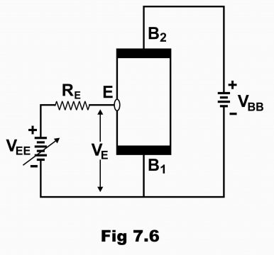
When the emitter enhances current IE above valley point, emitter voltages VE also increase slowly and the device starts operating as a positive resistor. It reveals that only E and B1 terminals are active terminals while B2 is a bias terminal (its function is just to provide outer voltages parallel to UJT). Unijunction transistor UJT characteristics are usually divided into three regions. The region located towards the left of the peak point is called the cut-off region, the region between the peak point and valley is called the negative resistance region while the region ahead of the valley point is known as the saturation region. Remember that a UJT can be brought into its conduction mode by providing an adequate pulse on its emitter and it can be reverted back to its OFF state by means of a negative trigger pulse. In other words, if the value of value of IE is lowered relative to IV, UJT turns off.
Characteristics Curves of Unijunction Transistor
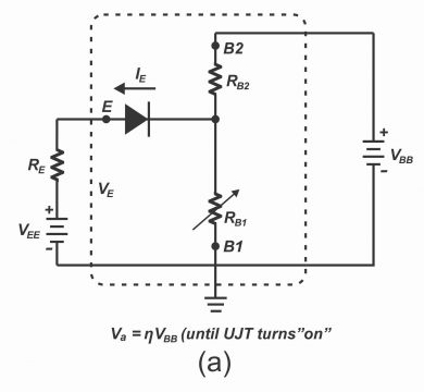
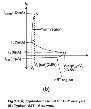
The circuit operation of a UJT has been revealed in figure 7.7 (A) by means of an equivalent circuit represented via dotted lines. For further clarification, UJT’s emitter-base (1) current-voltage (I-V) curves have also been demonstrated. If voltages parallel to B2 and B1 are considered constant, this curve represents changes within emitter current (IE) and emitter-base 1 voltage (VF). Names of different important points have also been written above the curve. Besides, important values have also been highlighted.
Figure 7.7 (A) Equivalent circuit for UJT analysis (B). Typical UJT I-V curve
OFF State
If we ignore the diode for a moment, one can understand looking at figure (A), that RB1 and RB2 assume the shape of such a divider, which produces voltages Vx on point x related to ground i.e.
VV = RB1/RB1+RB2 VBB = RB1/RBB VBB = ƞ VBB
Here ƞ reveals UJT’s voltage dividers’ intrinsic ratio RB1/RBB, which is called the intrinsic standoff ratio.
Voltages that are found on point x are a PN junction’s N side’s voltages. VEE is fitted with a source emitter, which is the P side of the junction. Thus, as long as the value of VEE is less than Vv, the emitter diode is reverse biased. This is off state of UJT, which has been depicted by an extremely low current region on the characteristics curve. A very high resistance exists on UJT’s E and B1 terminals during off conditions. The value of IE nearly equals a negligible reverse leakage current. Therefore, due to IE being negligible, the value of drop parallel to RE becomes zero, and the value of emitter voltage VE becomes equal to the value of source voltage (VEE)
As shown in the figure, the off state of unijunction transistor UJT actually expands to a point, where emitter voltage exceeds Vx by means of diodes’ threshold voltage (diodes internal junction voltage) VD (which are necessary for transmitting forward current through the diode). At the point P (as illustrated in the figure) emitter voltages are called peak point voltages. Its value is as follows
VP= VV+VD= ƞ VBB+ VD
Here the specific value of VD has been taken as 0.5 volts. For example, if ƞ=0.65 and VBB= 20V, then VP= 13.5V i.e.
VP= ƞ VBB+ VD = 0.65×20 +0.5 = 13.5V
Remember that value of peak point voltage (VP) also changes as a result of a change in VBB.
On-State
When VEE is increased gradually, unijunction transistor UJT remains off in the beginning, until when the value of VE is approx. equals VP, PN junction becomes forward bias and starts conducting in opposite direction. It must be kept in mind that the value of IF becomes positive near the peak point P on the I-V curve. When the value of VE equals exactly VP, emitter current equals IP (peak point current). At this point, heavily doped holes enter the N-type bar from the emitter (particularly in B1 region). N bar which is lightly doped provides very little opportunity for these holes to recombine. Thus, a lower half segment of the bar gets filled from superfluous current carriers (i.e. holes) and its resistance RB1 lowers intensively. As a consequence of a decrease in RB1, VV also drops. As a result of this drop, the diode becomes further forward biased and thus, IE rises further. An enhanced number of holes intrudes into B1 as a result of the high IE value. Consequently, RB1 diminishes further and thus this process moves on.
When this regenerative process comes to an end, the value of RB1 has reduced intensively till then (i.e. 5-25 ohm) and the value of IE rises extensively, which is controlled via extrinsic resistance RE. Thus, UJT enters into a low voltage but a high current region with respect to the I-V curve. The slope of this (on) region is quite linear, which depicts low resistance (as displayed by the figure). In this region, the value of the emitter’s voltage VE is comparatively lower (nearly 2 volts) but constant. Until IE’s values rise to their maximum rated value IE (sat). Thus, once UJT turns on, IE increases through an increase in VEE, while the value of VE remains about 2 volts.
Turning OFF the Unijunction Transistor
Once a UJT turns on, its emitter current mostly depends on VEE and RE. As VEE decreases, IE also shrinks along the ON segment of I-V curve. When IE drops to point V (valley point), the value of emitter current becomes equal to valley current (IV), which is basically that holding current, which is required to maintain a UJT ON. When the value of IE lowers than IV, UJT turns off and retreats back immediately to its OFF region on the I-V curve, where IE≈0 and VE=VEE.
Remember that value of valley current normally remains between 1-10 mA
Alternate Clarification
For further clarification, an equivalent unijunction transistor UJT circuit and characteristics curve have been presented in a simple manner vide figure 7.8. In figure (a), an equivalent circuit has been demonstrated along with its provided extrinsic emitter voltages VE. However, under such a case RB1 has been depicted as a variable resistance. If the value of VE is less as compared to the positive voltages (V1) provided parallel to RB1, then diode reverse biases. Reverse leakage current starts to flow from the diode when it gets reverse biased. This has been described by the curve on the left side in figure (b)
However, if VE is enhanced gradually, reverse bias diminishes, due to which reverse current also lessens. Until some further increase in VE ultimately leads to a complete stop on reverse bias and the value of reverse current also become zero. In such a situation, if VE is increased somewhat further, forward bias will kick-off. As a result, a very small quantity of forwarding current IE will start to flow from within emitter and base region 1. Thus, the resistance of this region subsides.
Figure 7.8 When VE is increased to VP= ƞ VBB+VD there is a sudden drop in the value of RB1
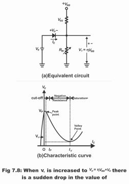
Now if a slight increase is made in forward bias, RB1 will decrease suddenly and extremely rapidly (value of RB1 reduces as a result of an increase in current and current increases further as a result of decrease in RB1 value, leading to a further fall in the value of RB1. Thus, a condition of sudden and quick reduction emerges). In other words, a regenerative operation takes place. That value of emitter voltage on which regeneration commences, is known as peak voltage VP (in other words, diode gets forward bias as a result of an added increase in emitter voltage and emitter current augments speedily. Consequently, excessive current starts to flow between the middle region of B1 and the diode. Thus, RB1‘s value reduces to an extremely low level, due to which emitter current also increases inordinately swiftly. This value of emitter voltage is known as peak voltage. This has been shown by VP in the figure. Thus, when the emitter’s voltage value increases and equals the total of V1 and forward drop found parallel to the diode (VD), it is called VP, as can be seen in figure a. i.e.
VP= ƞ VBB+VD
In figure (b) characteristics curve of UJT has been shown. Once when the value of emitter voltage (IE) increases and equals (VP), the emitter current rises (even if the IE value is reduced now) Emitter’s peak current (IP) flows towards the ground via RB1. In such a case, unijunction transistor UJT is termed ON. Due to the flow of IP via RB1, the number of charge carriers in RB1 enhances. As a result, its resistance slashes. In this region of the characteristics curve, UJT fires and emitter current rises excessively. Due to the transmission of a high emission current, a large voltage drop occurs parallel to the emitter’s resistance RE. Due to this VE reduces. Thus, emitter current augments whereas emitter voltage slashes after the device have fired. As a result, the negative resistance region forms (which has been shown on the right side of the peak point through a sloped curve in figure b) Negative resistance region continues until the emitter voltage reaches its minimum value. This minimum value of emitter voltage is called valley voltage and at the valley point, the value of the emitter’s voltage is at its minimum (as depicted vide figure b)
Resistance RB1 reaches its minimum possible value after the valley point which is called saturation resistance. In the saturation region, the emitter current can be increased further by increasing only the value of VE. After the valley point when IE is increased by a rise in VE, the device starts to operate as a positive resistance. In this region, the characteristics of a UJT are similar to a conventional forward-biased diode.
In short, the characteristics of a UJT can usually be divided into three regions. The region towards the left of the peak point is called a cut-off region. The region between the peak point and valley point is called the negative resistance region. Whereas region ahead of the valley point towards the right is known as the saturation region.
UJT is used as a voltage control switch. When its input voltage is increased and made equal to VP, it fires or turns ON. As a result, maximum current flows towards the ground from VBB. For turning the device off (or bringing it back into the cut-off region) emitter current IE value is reduced than the valley current IV.
Uses of Unijunction Transistor:
A unijunction transistor UJT can be used in several circuits due to its peculiar characteristics. Some of these are as follows:
1). Phase control
2). Switching
3). Pulse generation
4). Sine wave generator
5). Saw tooth generator
6). Timing and trigger circuits
7). Voltage or current regulator supplier
8). Stable multi vibrator etc.
UJT Relaxation or Saw tooth Oscillator
A unijunction transistor UJT can be used as a relaxation oscillator. In figure 7.9, a relaxation oscillator circuit consisting of a UJT has been exposed which operates as below:
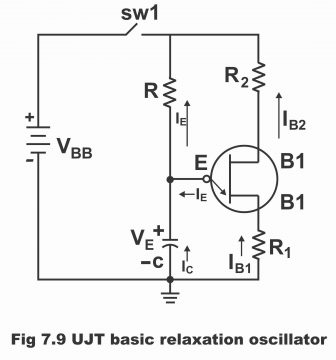
When a switch is turned on or closed, capacitor C starts charging via resistor R. This time of charging can be controlled by changing the value of R. The charging of a capacitor has been shown as wave forms in figure 7.10
Fig 7.10 waveforms for UJT relaxation oscillator
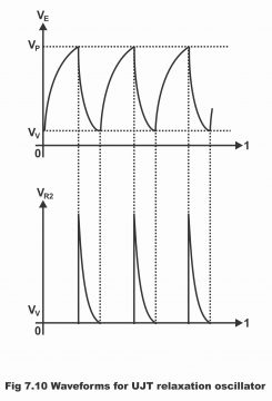
Capacitor voltages increase due to capacitor charging until their value reaches peak point value VP (in other words, a capacitor’s charging voltage reach UJT’s triggering voltage) As such a situation occurs, emitter diode or PN junction becomes forward bias and unijunction transistor UJT turns on (i.e. starts operating). As UJT turns on, the value of RB1 starts reducing to a very level (normally up to 10Ω). As the diode is now forward biased, therefore capacitor discharges via R1, RB1, and diodes’ low resistance route. In other words, negative resistance of UJT begins as soon as UJT turns on (in which emitter current IE enhances, however emitter voltage VE declines) and the capacitor starts discharging very briskly via forwarding biased junction.
When capacitor voltage reduces to valley point voltage VV, UJT turns off and capacitor restarts charging. After the capacitor having being charged, the repetition of the afore-mentioned procedure takes place automatically (i.e. above-mentioned operation takes place once again) and so long as the DC supply is received on the circuit, this operation also continues on. As a result, a saw tooth waveform is received (i.e. a saw wave is formed as a result of capacitors’ slow charge and a quick discharge) In order to calculate the frequency of this wave form, first of all, period of its cycle is ascertained (i.e. f= 1/T)
Remember that capacitor’s discharge time is quite less compared to its charging time and it is quite difficult to calculate discharge time because, at this time, UJT remains in its negative resistance region. As a result, resistance keeps on changing. The value of discharging time is usually ignored due to being quite low. The frequency of waves received from output depends on UJT’s stand of ratio (ƞ), capacitor C and resistance R. Frequency can also be changed by varying the value of R. Saw tooth waves received via relaxation oscillator can be utilized in oscilloscopes apart from SCR firing. Further, saw tooth voltage waves can normally be used as sweep voltages on TV receivers’ picture tubes.
In order to work efficiently with an oscillator mentioned above, the fulfillment of the following 2 conditions are essentially related to the on /off of a UJT unijunction transistor.
1). In order to turn a UJT on in a definite manner, the IE value should not be confined related to IP (IE value should not be less than IP otherwise UJT will not turn on)
2). For turning a UJT off certainly at a valley point, the value of R must be so high value of IE lessens as compared to the value of IV at the valley point (in other words, the value of drops parallel to R at the valley point must be less than IV R)
Thus, for turning a UJT on or off in a reliable manner, the value of R should be in the following range
VBB-VP/IP >R>VRB-VV/IV
Alternative Explanation of UJT Saw Tooth Oscillator
A saw tooth circuit comprising a UJT has been displayed in figure 7.11. This circuit comprises a power source (or a dc supply) a unijunction transistor and an R-C network. The functioning process of the circuit is as follows:
When switch S is closed at the start, the following factors occur
1). A low current value starts to transmit through R1 and R2 via B1 and B2 and an initial reverse bias sets up parallel to the E/B1 junction.
2). Meanwhile (i.e. as soon as switch S closes) capacitor C starts charging via RE and voltages parallel to it, begin to increase.
3). When capacitor voltages equal emitter firing voltage or peak point voltage VP, then the E/B1 junction turns forward biased and the emitter enters the negative region of its characteristics.
4). E/B1 junction offers very little resistance due to being forward biased, thus capacitor C starts to discharge via B1 and R1. Remember that the discharge ratio of C is determined through the E/B1 junction and R1.
5). As soon as capacitor voltage becomes zero, the E/B1 junction reverses bias again and thus stops conducting.
6) Thus, the initial status of circuits’ operation recurs once again due to which C starts to charge and the full circuit cycle or circuits’ entire factors tend to repeat.
Figure 7.11 (a) Figure 7.11 (b) a UJT relaxation oscillator
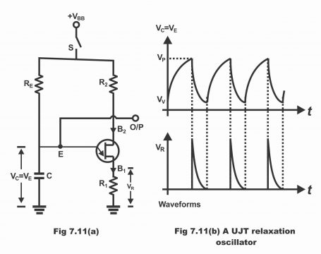
Wave forms of an emitter voltage have been demonstrated in figure (b). It is evident from the figure that capacitor C charges via RE, until capacitor C, reaches voltage VP. At that time, the UJT junction turns on via E/B1 or it does conduct and the capacitor starts discharging via emitter. As RE’s value is immensely high (10K or even higher), therefore charging ratio is relatively slow. Due to a very low RE value (50Ω or even less) discharging function occurs extremely quickly. Thus, as a result of slow charge and rapid discharge of a capacitor, a saw tooth wave generates.
Once when the capacitor has been discharged, Unijunction transistor UJT retreats to its off status owing to the emitter’s current value getting less than IV. Then the capacitor starts recharging and the full cycle is repeated. Resisting capacitor voltage and output wave forms have been illustrated in figure (b). These types of oscillators are applied in synchronized circuits for control purposes by means of generating trigger and timing pulses.
Previous Topic: Triac construction, Working, and Uses
Next Topic: Light Activated SCR or LASCR
For electronics and programming-related projects visit my YouTube channel.
Discover more from Electronic Clinic
Subscribe to get the latest posts sent to your email.


Great post! I found the explanation of the UJT’s construction and working principles really insightful. It’s fascinating to see how solid-state devices like this have evolved and their practical applications. Appreciate the clarity in your writing!
This blog post on the Unijunction Transistor (UJT) was incredibly insightful! I appreciated the detailed explanation of its construction and how it operates as a solid-state device. The diagrams helped clarify complex concepts, making it easier to grasp. Looking forward to more posts like this!